Introduction
In modern high-performance graphics cards and CPUs, the stability and purity of the core voltage in Vertical Direct Power (VDP) systems are paramount. The Power Management ICs (PMICs) or Voltage Regulator Modules (VRMs) used in such systems are responsible for efficiently and accurately converting the 5V supply from the motherboard to around 1V core voltage, while needing to withstand extremely high current loads. The LGA72-1.1 test socket, specifically designed for this purpose, provides an integrated validation platform that simultaneously supports both testing and aging for these high-current power delivery chips, representing a critical step in ensuring end-product reliability.
Technical Challenges in Testing LGA72 Chips
1. Extremely High Current Load Requirements
In a Vertical Power Delivery architecture, each power phase must carry a significant current. Consequently, each pin of the corresponding PMIC or VRM chip may need to handle a continuous current of 3-5A. This places extreme demands on the test socket’s contact impedance, current-carrying capacity, and resistance to electromigration.
2. Verification of Conversion Efficiency and Accuracy
Converting a 5V input to a 1V core voltage implies a substantial 80% voltage drop. In this process, the chip’s conversion efficiency (e.g., the difference between 95% and 97%) and voltage regulation accuracy (Load Line Regulation) directly impact system efficiency and stability. The test socket must provide very low contact resistance and excellent signal integrity to ensure the authenticity of measurement data.
3. Severe Thermal Management Challenges
According to Joule’s Law (P = I² * R), even milliohm-level contact resistance between the test socket and the chip pins can generate significant heat during high-current testing. Inadequate heat dissipation will lead to parameter drift, thermal damage to the chip, or a drastic reduction in the test socket’s own lifespan.
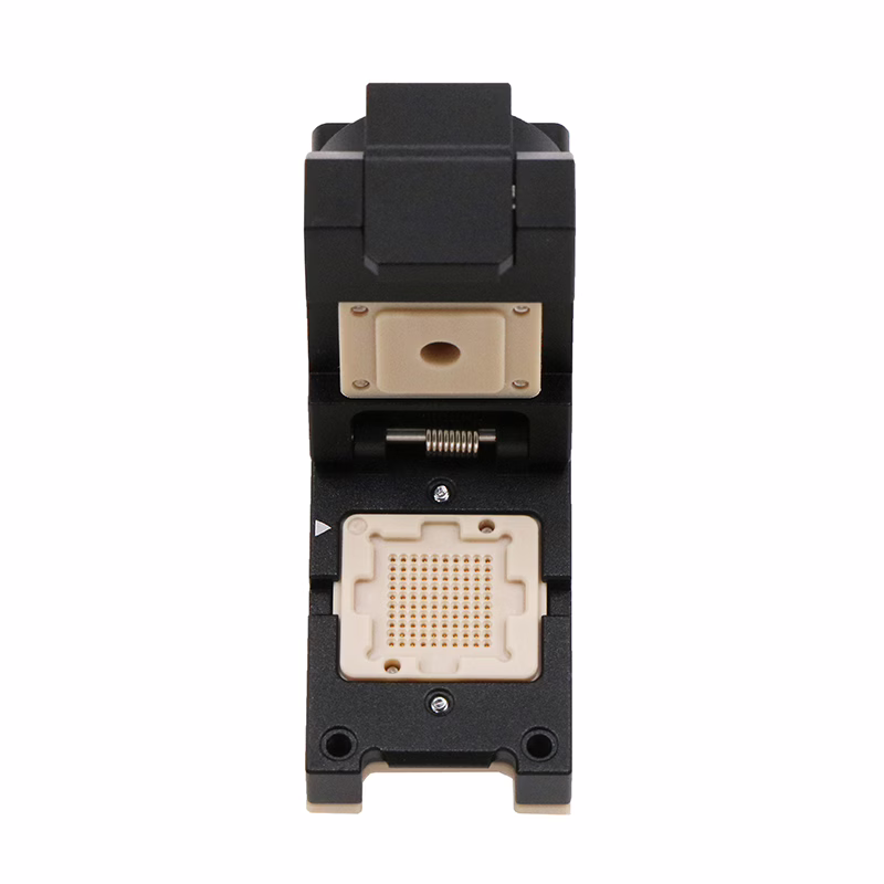
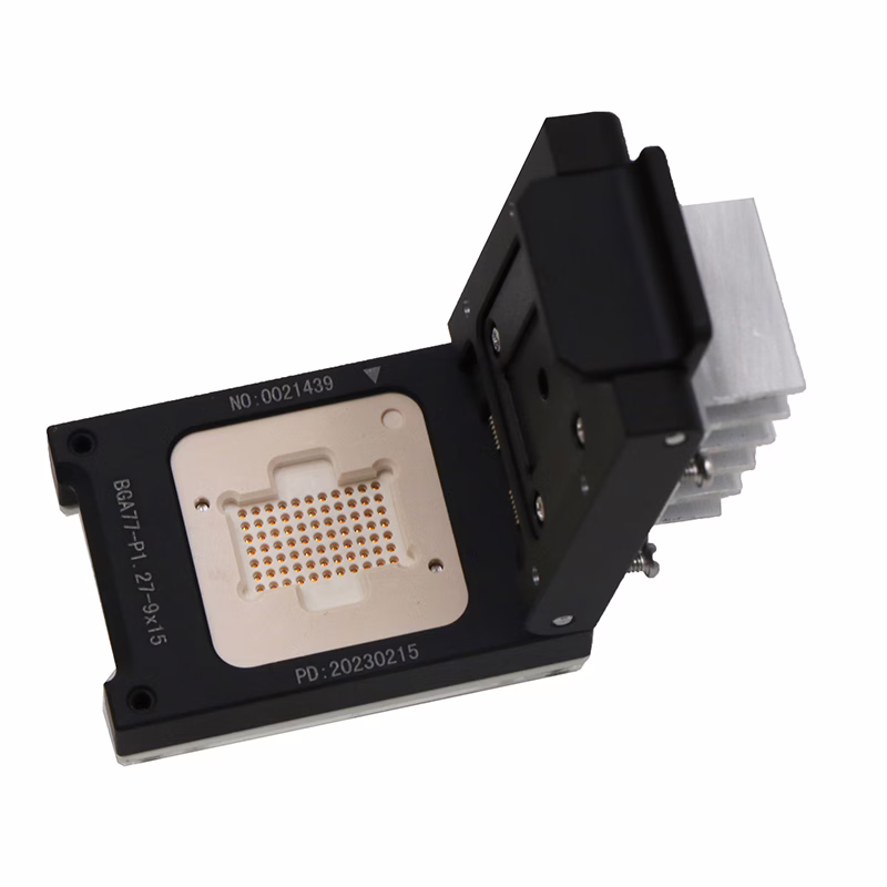
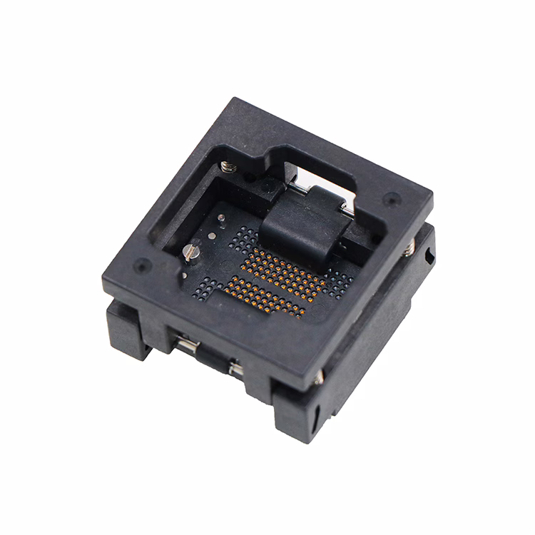
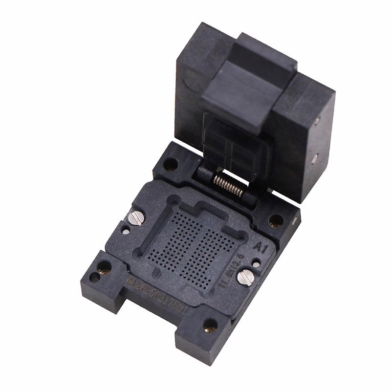
Core Technical Features of the LGA72-1.1 Test Socket
1. Contact Design Optimized for High Current
- High-Performance Alloy Contacts: Uses special beryllium copper or palladium cobalt alloy spring contacts, combining high conductivity, high elasticity, and resistance to stress relaxation, ensuring stable long-term contact for each pin under 3-5A currents.
- Low Contact Resistance: Through precision machining and surface plating (hard gold), the contact resistance per pin is maintained below 10mΩ, reducing heat generation at the source.
2. Integrated Efficient Thermal Solution
- Thermally Conductive Body: The socket body uses high-thermal-conductivity engineering plastics or metal substrates, with integrated heat dissipation fins to quickly draw heat away.
- Active Cooling Compatibility: Features standard mounting holes for easy integration of fans or Peltier coolers, enabling active temperature control to handle chip power dissipation exceeding 30W during testing.
- Optimized Thermal Path: A flat heatsink mounting surface on the top of the socket ensures the shortest possible path for heat generated by the chip to be removed.
3. Integrated Dual-Mode Design for Testing and Aging
The LGA72-1.1 test socket supports a complete validation workflow on a single platform:
- Engineering Test Mode: Used for initial functional verification, parametric characterization (e.g., efficiency curves, transient response), and performance binning.
- Aging/Burn-in Mode: Supports long-duration (e.g., 48-168 hours) reliability testing under high temperature (e.g., 85°C-125°C) and full load current to screen out early failure products.
Key Performance Parameters
| Parameter | Specification | Remarks |
|---|---|---|
| Max Current Carrying Capacity | 5A / Pin | Continuous operation, no derating |
| Operating Voltage Range | 0 – 6V | Covers 5V input & 1V output monitoring |
| Contact Resistance | < 10 mΩ | Per pin, typical value |
| Operating Temperature Range | -40°C to +125°C | |
| Thermal Dissipation Capability | Supports chip power > 30W | Requires active cooling system |
Application Solutions and Implementation Process
Recommended Test Flow
- Contact Impedance Check: Automatically measure the contact resistance of each pathway to ensure good connection.
- Static Functional Test: Verify basic voltage conversion functionality, enable/disable logic.
- Dynamic Performance Test: Scan conversion efficiency, output voltage ripple, and load regulation under different load currents (0 to Amax).
- Transient Response Test: Apply rapidly changing loads to test the chip’s response speed and overshoot/undershoot.
- Accelerated Aging Test: Perform long-term stress testing under high temperature/humidity with maximum operating current, monitoring parameter drift.
Phased Thermal Management Strategy
- Low-Power Testing (<10W): Relies on the passive cooling capability of the test socket itself.
- Medium-Power Testing (10-20W): Enable low-speed forced air cooling.
- High-Power/Aging Testing (>20W): Must enable high-speed forced air or liquid cooling systems, with real-time monitoring of the chip junction temperature.
Advantage Summary
The core advantages of the LGA72-1.1 test socket are:
- High Reliability: Reinforced design for high-current scenarios ensures long-term repeatability and accuracy of tests.
- High Integration Level: Integrating testing and aging functions into one unit improves test efficiency and reduces equipment investment and changeover costs.
- Flexible Thermal Configuration: Scalable cooling solutions allow adaptation to varying stringent requirements from engineering validation to mass production screening.
- Easy Integration: Standardized mechanical and electrical interfaces enable quick connection to Automated Test Equipment (ATE) and burn-in board systems.